

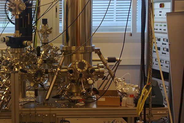
This scanning tunnelling microscope (STM) features a base temperature of 1.2 K and an axial magnetic field of 3 Tesla. At LMA, we have implemented the option of spin-polarized STM which allows us to image simultaneously the magnetic moment and the topography with atomic resolution. The facility is attached to a multichamber sample preparation system under UHV (P<1E-10 mbar) which can deal with any kind of surface.
The system can host up to 24 samples/tips, 7 e-beam metal evaporators (two of them focused to the STM head in cryogenic conditions), and two resistive evaporators for organic materials.
This facility is fully compatible with all standard STM related techniques, but thanks to its unique specifications, the instrument is specifically devoted to magnetic characterization of surfaces and high-resolution spectroscopy (0.08 meV). It is worth noticing that both of them can be combined with STM manipulation to construct atomically precise nanostructures.

Microscopy and tunneling spectroscopy:
- Structural and electronic characterization with atomic resolution.
- High resolution structural characterization using tips functionalized with CO.
- Characterisation of band structure in reciprocal space using quasiparticle interference patterns
Magnetic measurements:
- Spin-polarised STM in constant current/height mode.
- Continuous measurement of magnetic contrast as a function of applied external field. Hysteresis cycles and individual spin magnetisation curves.
- Spectroscopy of low energy excitations such as inelastic spin-flip and Kondo effect.
- Non-collinear magnetic ordering.
- Temperature range: 1.2 to 10 K (Joule-Thompson refrigerator)
- Magnetic field: Dry-split coil providing an axial field up to 3 Tesla (maximum rate 0.1 T/min).
- LHe hold time: 100 hours
- LN2 hold time: 80 hours
- Z topographic noise: 1-2 pm peak-peak; <500 fm/(Hz)^(1/2)
- In-situ tip exchange.
Sample preparation: 3 ion-guns, 3 e-beam heaters (100-1300ºC). 1 flash heater (>2000 ºC in 25 seconds), low energy electron diffraction and Auger spectroscopy (SPECS ErLEED 150), quadrupole mass spectrometer for residual gas analysis, 7 leak-valves for controlled gas injection, 1 SPECS EBE4 and 3 SPECS EBE1 e-beam evaporators, 2 parking stations for mini-UHV transportable organic evaporators, 1 high temperature effusion cell (CreaTEc).
Examples of work that can be done

Fig 1. The striped pattern corresponds to the antiferromagnetic spin spiral of Mn on W(110), as imaged with a Fe-coated W tip. Following the magnetic contrast as a function of the applied field, it is possible to retrieve single atom magnetization curves, as is the case of the tip apex magnetization shown in the bottom left graph. The red dots are spin resolved d orbitals of Co atoms with different magnetization directions.

Fig 2. Atomic scale memory consisting in a chain of 7 Co atoms built with the STM tip over a NaCl patch grown on top of Cu2N/Cu001. The left graph shows the associated low bias spectroscopy taken at 1.18 K with a modulation of 80 eV.

Fig 3. The middle panel shows the Fourier transform of the backscattering pattern of electrons in the topological surface state of Bi2Te3, taken at an energy slightly above the Dirac point (right panel shows the theoretical iso-energy slice of the Dirac cone). This scattering of the fully spin polarized topological current is enabled by the magnetic moment of individual Co atoms deposited on the surface.
Advanced Microscopy Laboratory
We are a unique initiative at the national and international level. We provide the scientific and industrial community with the most advanced infrastructures in electron microscopy and local probe microscopy for the observation, characterization, nanostructuring and manipulation of materials at the atomic and molecular scale.
Contact information
Campus Río Ebro, Edificio Edificio I+D+i

Direct Links
© 2021 LMA | Website developed by o10media | Política de privacidad | Aviso legal | Condiciones de uso | Política de Cookies |