

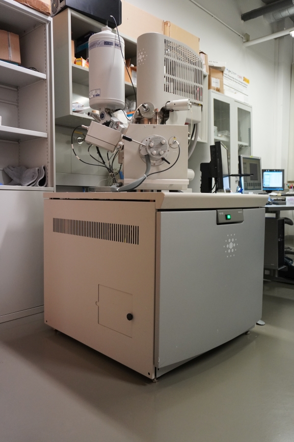
InspectF50A scanning electron microscope (SEM) is a type of electron microscope that produces images of a sample by scanning it with a focused beam of electrons. The electrons interact with the sample, producing various signals that can be detected in the electron microscope detectors giving information about surface topography and composition of the sample.
The Inspect F-50 SEM instrument is a general-purpose field-emission Scanning Electron Microscope for imaging and composition analysis by energy-dispersive X-ray microanalysis (EDS).
The expertise of our scientific and technical staff is also offered to researchers from public and private research centers and also to professionals from industrial sectors that require the use of this instrument.

- What kind of information can be obtained with this instrument?
- Sample requirements
- Technical Specifications
Image / Analysis
By using the different SEM Detectors with which this instrument is equipped, the following information can be obtained:
- Images with secondary electrons image and topography by means of an ETD (Everhart-Thornley Detector).
- Image and composition by using a BSED (Back Scattering Electron Detector).
- Elemental chemical analysis by means of Energy-dispersive X-ray spectroscopy (EDX).
Liquid and non-conductive samples observed need to be dried and metallized prior to observation. Samples studied at low vacuum can be used without metallization at low voltage (low contrast and low sharpness images).
Types of samples that can be studied with Inspect F-50 SEM include:
- Conductive and non-conductive samples, bulk, films, coatings, powders (compacted), etc.
- Samples compatible with high vacuum conditions.
- Sample Diameter from less than 1 mm up to 50 mm.
Inspect F 50 |
||
SEM |
15 kV |
20.0 nm |
Maximum beam current |
200 nA |
|
Vacuum |
Modes |
High Vacuum |
X x Y x Z (mm) |
50 x 50 x 50 mm |
|
Stage |
Tilt angles |
-15º to 75º |
Rotation |
360º |
|
Detection |
Solid state BSE |
BSED |
ETD |
SE |
|

Laboratorio de Microscopías Avanzadas
We are a unique initiative at national and international levels. We provide the scientific and industrial community with the most advanced infrastructures in Nanofabrication, Local Probe and Electron Microscopies for the observation, characterization, nanopatterning and handling of materials at atomic and molecular scale.
Contact information
Campus Río Ebro, Edificio Edificio I+D+i

Direct Links
© 2021 LMA | Website developed by o10media | Política de privacidad | Aviso legal | Condiciones de uso | Política de Cookies |