

Additionally, the tip can be functionalized with CO molecules, which provides intra-molecular resolution. As a bonus, the AFM can work on insulating or semiconductor surfaces without current exchange.The equipment has an attached preparation chamber to clean metal substrates and evaporate both organic and inorganic materials, which can be characterized by a low energy electron diffractometer (LEED). It has a chamber for rapid entry of substrates that allows exfoliation.The research lines are oriented to the study of molecular interactions, self-assembled systems, and electronic and structural properties determination of hybrid films composed of metal-organic compounds.

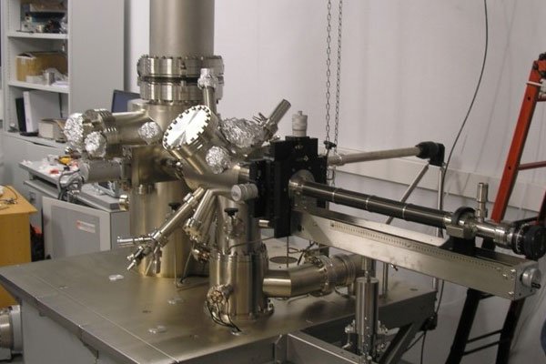
Scanning tunneling microscopy and spectroscopy:
- Structural and electronic characterization with sub-molecular resolution.
- Band structure characterization in reciprocal space by means of quasiparticle interference patterns.
- High-resolution structural characterization using CO functionalized tips.
- Tip manipulation of atoms and molecules.
Atomic force microscopy:
- Study of all types of samples: from insulating to metallic.
- Simultaneous recording of forces and conductance.
- Map acquisition of electronic charge (surface potential) down to the sub-molecular scale.
-
Temperature range: 4.7 K, 78 K and 300 K
-
LHe / LN2 hold time: 62 /48 hours
-
Z topographic noise: 3 pm peak-peak; <500 fm/ÖHz
-
Energy /force resolution: 1 mV / 1 pN
-
Minimum stable Qplus oscillation: 20-30 pm
-
In-situ tip exchange.
-
Quick cooling and stabilization of the piezo
-
Maximum sample size: 3 mm thick and 10 mm wide.
Combined resistive heating and LN2 cooling manipulator (temperature range 100 – 1100 K). Low energy electron diffraction equipment (LEED), mass spectrometer (quadrupole) for detection of residual gases, 2 ion guns, 4 leak valves for controlled gas injection, 1 metal evaporator (e-beam) and 2 organic evaporators (resistive heating). Accessory pumping stations. Carrousel with capacity for up to 4 samples.

Figure 1: Extended DCA/Cu(111) metalorganic network. Panel a) is a 50x50nm2 zoom of panel b), which is a 300 x 300 nm2 image with the network grown on it. This array is grown by deposition at RT of the 9,10-dicyanoanthracene (DCA) molecule shown in panel c). It extends over many different steps and exhibits a single domain and is particularly stable since high tunneling currents can be used to scan the sample. d) LEED pattern of the network showing an 8×8 structure with respect to the substrate. STM Image parameters: Vbias=1.5V; It=200nA. LEED parameters: E = 20 eV, sample at RT.


Figure 3: On-surface synthesis of MnDCDAE molecule on Ag(001). The structure is formed by four molecular precursors surrounding a single Mn atom that polymerizes into a phthalocianine structure. The larger molecule looks like a cross when visualized by STM (central image), but shows up the sub-molecular details when a CO functionalized tip is used(right image).
Laboratorio de Microscopías Avanzadas
We are a unique initiative at national and international levels. We provide the scientific and industrial community with the most advanced infrastructures in Nanofabrication, Local Probe and Electron Microscopies for the observation, characterization, nanopatterning and handling of materials at atomic and molecular scale.
Contact information
Campus Río Ebro, Edificio Edificio I+D+i

Direct Links
© 2021 LMA | Website developed by o10media | Política de privacidad | Aviso legal | Condiciones de uso | Política de Cookies |