DUAL BEAM
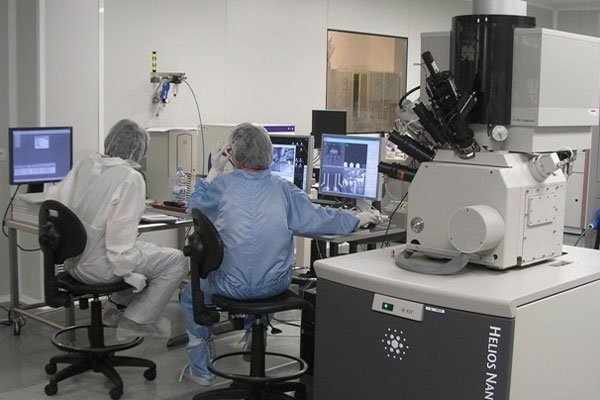
The focused electron and ion beam lithography is a mature technology, used in industry and at laboratory level since the last 20 years. This technology plays nowadays a major role in the context of Nanotechnology. The underlying technology supporting focused electron and ion based equipments relies on the use of field-emission electron and ion sources, the electron and ion acceleration up to tens of kV and their focusing and scanning on the area of interest.
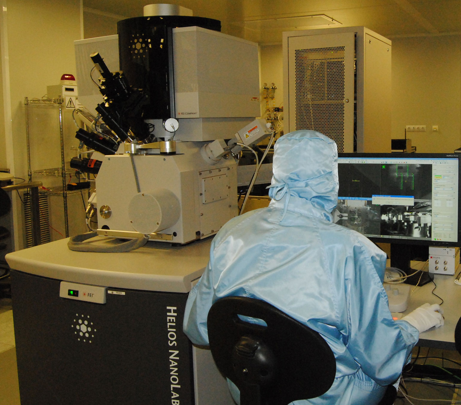
Currently, electron beams focused to 1 nm and ion beams focused to 5 nm integrate the state-of-the-art electron and ion columns devoted to nanolithography. Together with dedicated electron or ion beam equipments, another option is to combine both types of columns in a single instrument, which is coined dual beam or cross beam, depending on the supplier.

Those equipments have normally additional parts such as gas injectors, nanomanipulators, etc., which constitute a nanolaboratory with many applications in Nanotechnology. In particular, the preparation of thin lamellae for subsequent analysis in a Transmission Electron Microscopy (TEM) has become a routine task, with large impact at the Semiconductor industry as well as at the laboratory level. By using cryo-transfer set-ups, it is possible to study frozen samples, which is extremely useful in certain applications.
On the other hand, the use of environmental SEM is of great interest in life sciences as charging effects are minimized and biological samples can be studied in the right conditions of humidity without degradation.
The LMA is a unique opportunity for the development of this field.
Several researchers from the local research institutes (INMA, I3A, IUCA, ICB, etc.) develop research lines using the described dual beam and environmental SEM equipments. The SEM, XRD and XPS-AES equipments serve as additional support to these investigations. Hereafter, a brief summary of those research lines are included:

In the dual beam equipments for lamellae preparation and nanolithography:
- Lamellae preparation for subsequent TEM investigation of their physical and chemical properties This activity is carried out by the researchers from the Thin Film Growth laboratory working on Spintronics and Caloritronics applications as well as by the TEM group, whose activities are later described.
- Nanoelectronics and Spintronics based on 2-dimensional systems and quantum materials such as graphene and bismuth-based films, with high carrier mobility and long spin diffusion length.
- Magnetic nanostructures based on cobalt and iron grown by focused electron beam induced deposition for applications in magnetic information storage, logics and sensing.
- Superconducting nanostructures based on W nanodeposits grown by focused ion beam induced deposition for studies of low-dimensional superconductivity and fabrication of nanoSQUIDs.
- Magnetic properties of antidot networks fabricated by electron beam lithography and focused ion beam.
- Fabrication of nanocalorimeters for magnetic refrigeration with molecular magnets.
- New superconducting SQUID sensors for ac susceptometry and study of qubits in the mK range.
- Making electrical contacts using the Cryo-FIBID technique.
- Electron and ion irradiation of palladium-based metal-organic films for nanoelectronics applications.
In the equipments concerning life science dual beam and environmental SEM:
- Thermosensitive hidrogels based on dendritic macromolecules derived from Pluronic®. These systems are interesting for tissue regeneration. Supramolecular hidrogels based on glicolipids modified with photosensitive groups. These systems are interesting as carrier agents sensitive to light stimulii.
- Studies of hyperthermia using magnetic nanoparticles. Currently, dendritic cells are being cultured with magnetic nanoparticles for Trojan horse approach to cancer treatment.
- Efficient biosensing using different strategies for the biofunctionalization of metallic nanoparticles and the chemical modification of enzimes and proteins as recognition reagents.
- Nanotherapy using multifunctional biofunctionalized nanoparticles. By using inorganic nanoparticles and organic ligands biologically active, research focuses on cancer therapy.
- Morphology and metastructure resulting from the interaction between cells and nanoparticles, with applications in neuron regeneration, magnetotransfection, magnetic hyperthermia and controlled drug delivery.
- Nanoparticle internalization inside vegetal cells for basic studies of transport in plants as well as studies of advanced treatments on plants.
The described research activities are at the frontline in several fields and the involved groups are competitive at the national and international level as can be deduced from the outstanding funding obtained from European programs calls and national project calls.
Laboratorio de Microscopías Avanzadas
We are a unique initiative at national and international levels. We provide the scientific and industrial community with the most advanced infrastructures in Nanofabrication, Local Probe and Electron Microscopies for the observation, characterization, nanopatterning and handling of materials at atomic and molecular scale.
Contact information
Campus Río Ebro, Edificio Edificio I+D+i
Direct Links
© 2021 LMA | Website developed by o10media | Política de privacidad | Aviso legal | Condiciones de uso | Política de Cookies |


