Molecular Electronics
From single molecule devices to ordered 2D molecular networks, organic and metalorganic complexes are expected to play a leading role in future nanoscale electronic devices, overcoming production and technical constrains of nowadays CMOS technology. The idea behind it is to control the functionality of an ensemble of molecules by carefully designing the structure of its individual molecular constituents. The versatility of organic synthetic chemistry provides an almost unlimited pool of molecular building blocks. In this way, the natural advantages of molecular electronics such as easy miniaturization and low power consumption, are enhanced by the capability of programming their response to different physical stimuli, which will determine its application as organic transistors, photovoltaic cells, gas sensors, membranes for biological filtering or even quantum bits.
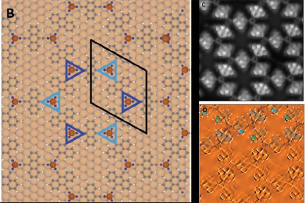
At the SPM labs of LMA there are two different approaches to molecular electronics. The first one consists in the sublimation of molecular precursors under UHV conditions that react onto a metallic surface and form molecular species that cannot be synthesized by standard wet chemistry. Examples of this are individual magnetic metal-Phthalocyanine cores with ligands capable of undergoing a photon induced reversible electrocyclic reaction, or crystalline metalorganic coordinated networks with the peculiar threefold structure of an organic topological insulator, as the one illustrated in the Figure below:

B) Schematic illustration of a Kagomé lattice where the appearance of topologically protected electronic bands are predicted (atoms grey=Carbon, white=Hydrogen, blue=Nitrogen, brown=Copper). C,D) Realization of such lattice imaged by bond-resolving STM with CO-functionalized tip, the atomic model of the lattice is overlaid on D panel image.
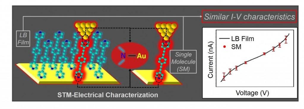
The second one consists in the characterization by AFM and STM in ambient conditions (pressure and temperature) of the morphology and transport properties of individual molecules and monolayers on Au-based electrodes and also on carbon-based electrodes. The length of the molecular backbone, the dopants and the end groups to immobilize the molecule in the electrode are the variable parameters in these studies. In particular we are working on the fabrication of robust metal-molecule junctions, deposition of the top contact electrode, and electrical characterization of metal-molecule-metal junctions and monolayers deposited by self-assembly, Langmuir-Blodgett or electrografting methodologies. In this figure, we provide an artist view illustration of the fabrication and measurement process of single molecule I(V) characteristics.

We record I-V characteristics by forming short lived bonds between the tip apex and the molecules, using thereby the tip as sort of atomically precise electrical probe. Characteristics of molecular arrays in LB films and single molecules fished over the surface are compared to validate the results.
Laboratorio de Microscopías Avanzadas
We are a unique initiative at national and international levels. We provide the scientific and industrial community with the most advanced infrastructures in Nanofabrication, Local Probe and Electron Microscopies for the observation, characterization, nanopatterning and handling of materials at atomic and molecular scale.
Contact information
Campus Río Ebro, Edificio Edificio I+D+i
Direct Links
© 2021 LMA | Website developed by o10media | Política de privacidad | Aviso legal | Condiciones de uso | Política de Cookies |


