SPINTRONICS
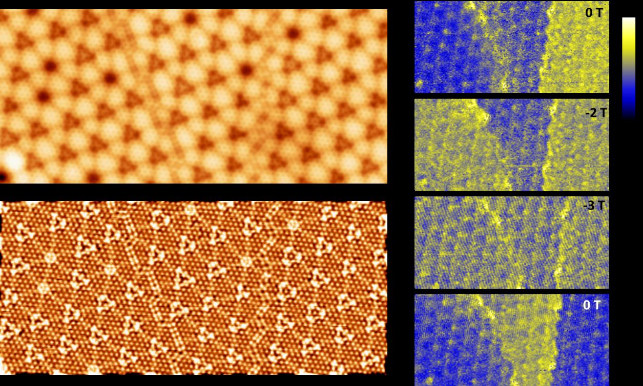
We are interested in spin dependent transport and spin-spin interactions at the smallest conceivable scale, like single atoms, individual metalorganic complexes or nanostructures consisting in a few hundreds of atoms. Our goal is to set the basis for the design and understanding of optimized active elements for their implementation in atomic scale functional devices and to achieve maximum energy efficiency in them. For this purpose, the spin-polarized STM technique grants us access to the spin density of a surface with atomic resolution. By performing SP-STM as a function of temperature, external magnetic field and tunnelling energy, we can disclose in detail the magnetic ground state of a test sample. Then the electronic transport across minute regions with known spin contrast can be understood. The figure below illustrates this concept with atomic scale structuralantiphase-boundaries appearing in monolayer GdAu2 soft ferromagnet, which induce a clear antiferromagnetic coupling between neighbouring structural domains.

Left column) Atomically resolved STM image of the GdAu2 monolayer with different contrasts, emphasizing the structure of the two visible antiphase boundaries. Right column) Sequential series of spin-polarized STM images showing the evolution of the in-plane spin as a function of magnetic field.
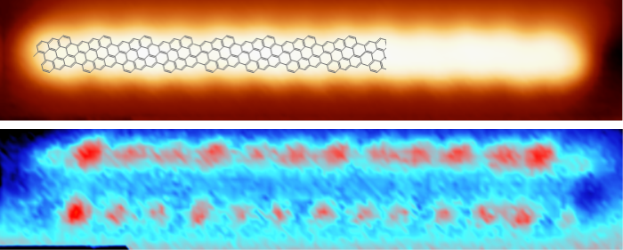
In the last years, we have also turned our attention to spin transport in graphene nanostructures The graphene nanostructures are prepared by on-surface synthesis from designated molecular precursors that react on the surface to yield the desired products. We have focused in the magnetic and transport properties graphene nanoribbons with zig-zag terminated edges, which constitute a paradigmatic example of a semiconducting internal behaviour together with 1D metallic states hosted by the carbons at the ribbon’s edge. The edge metallic states can develop large spin polarization.

Caption: Topography and simultaneous dI/dV map carrying the local density of states (energy=-690 meV) of a graphene nanoribbon with an edge composed by repeated blocs of 3 zig-zag and 1 arm-chair segment. The 1D edge state at the ribbon’s edges is clearly visible. The state of the 1D edge at the edges of the tape is clearly visible.
Laboratorio de Microscopías Avanzadas
We are a unique initiative at national and international levels. We provide the scientific and industrial community with the most advanced infrastructures in Nanofabrication, Local Probe and Electron Microscopies for the observation, characterization, nanopatterning and handling of materials at atomic and molecular scale.
Contact information
Campus Río Ebro, Edificio Edificio I+D+i
Direct Links
© 2021 LMA | Website developed by o10media | Política de privacidad | Aviso legal | Condiciones de uso | Política de Cookies |


