

The Dual Beam Helios 600 model consists of a 30 kV field-emission scanning electron column and a 30 kV Ga focused ion beam placed at 52º one from each other. The ion column is able to work properly at low voltage (5 kV and lower), allowing the preparation of lamellae with low ion damage. In this equipment, there are five gas injectors which allow the growth of nano-deposits with high resolution, such as W-based superconducting nano-deposits with lateral size of 40 nm and Co-based ferromagnetic nano-deposits with a lateral size of 30 nm. These ultranarrow dimensions are at the forefront of research in these topics. In this equipment, there are five gas injectors which allow the growth of nano-deposits with high resolution, such as W-based superconducting nano-deposits with lateral size of 40 nm and Co-based ferromagnetic nano-deposits with a lateral size of 30 nm. In addition, electrical microprobes (Kleindiek®) could be placed inside the chamber for in-situ electronic transport measurements; electron beam lithography is also possible thanks to a Raith® software/hardware.

Both instruments are working properly for the requested main tasks, i.e., lamellae preparation, cross-section imaging, nanolithography based on ion patterning, ion/electron nanodeposition, electronic transport measurements and electron beam lithography (Raith® software/hardware).
Image (resolution 1.4 nm)/ Analysis:
By using the different detectors available within these instruments, the following information can be obtained:
- Image with secondary electrons and topography by means of an ETD/TLD (Everhart-Thornley Detector / Through Lens Detector).
- Image (back scattered electrons) and composition by using a BSED (Back Scattering Electron Detector).
- Images of secondary ions sensitive to crystallographic direction by using CDEM/ICE (Channel Detection Electron Multiplier / Ion Conversion and Electron) detectors.
- Elementary Chemical Analysis by EDX (Energy-Dispersive X-ray micro-analysis).
- STEM (scanning-transmission) images.
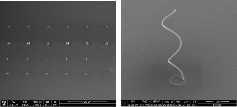
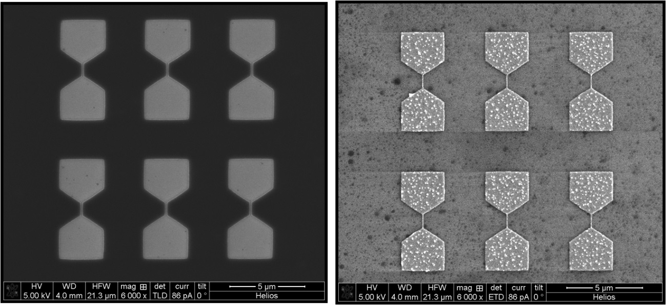
Nanofabrication(lateral dimension between 50 nm and tens of microns):
- Direct FIB: focused ion beam; etching of a predesigned motif over the sample.
- Directa FEBID/FIBID(focused electron/ion beam induced deposition).
GASES PRECURSORES
(CH3)3(CpCH3)Pt, Co2(CO)8, W(CO)6, TEOS + H2O –> SiO2, Selective Carbon Mill
(MgSO4•7H20), I2, XeF2
- Indirect: e-beam lithography (Raith®).
Micromanipulation
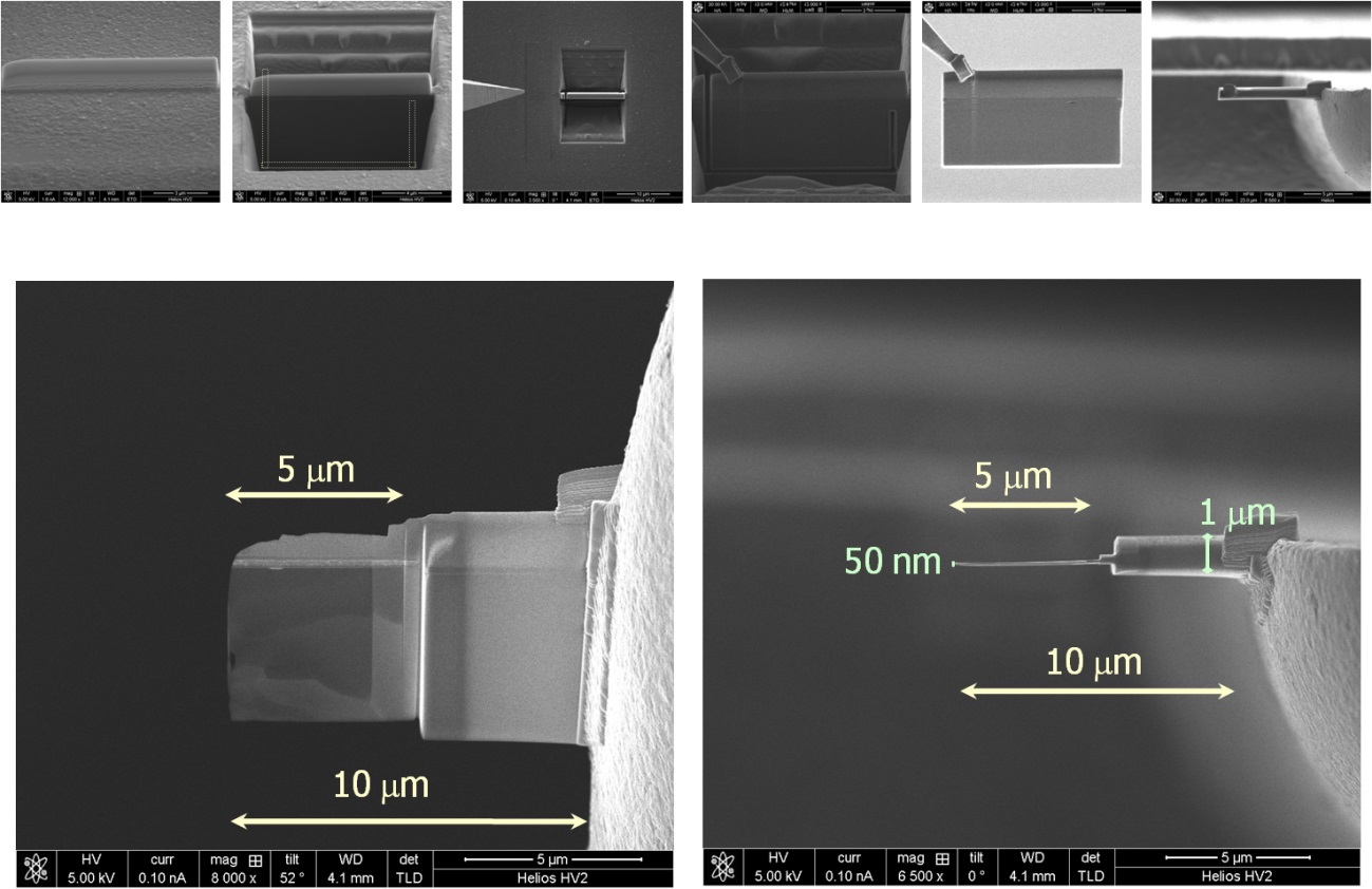
- Lamellae preparation for TEM observation– Omniprobe®.
- Micro-tweezers (Kleindiek®).
In‐situ electrical measurements
- 4 Microprobes Kleindiek®.
- Non-conductive samples must be coated with a conductive material (by sputtering or evaporation, which can also be done in our Centre).
- Conductive and non-conductive samples as bulk, films, powder (compacted), etc. can be studied.
- Samples should be compatible with high vacuum conditions.
- Dimensions of the samples: less than 1 mm to 100 mm (sample height < 10 mm).
IMAGES
ResolutionElectron beam |
0.9 nm at 5 kV |
ResolutionIon beam |
4.0 nm at 30 kV |
Voltage rangeLanding |
E-beam: 20 V – 30 kV-beam: 500 V – 30 kV |
Probe current |
E-beam: 0.8 pA up to 26 nAI-beam: 0.1 pA – 65 nA (15 position aperture strip) |
High Precision5-axesmotorizedstage. |
XY: 150 mm, piezo-drivenZ: 10 mm motorizedT: – 10° to + 60°R: n x 360° (endless), piezo-drivenTilt accuracy (between 50° to 54°): 0.1°Compucentric rotation and tilt |
Chambervacuum |
< < 2.6*10-6 mbar (after 24 h pumping) |
Samplesize |
Maximum size: 150 mm diameter with full rotation (larger samples possible with limited rotation)Weight: max. 500 g (including the sample holder) |
Growth of nano-deposits with high resolution:
EBL: electron beam lithography (Raith® software/hardware)
Electrical microprobes (Kleindiek®)
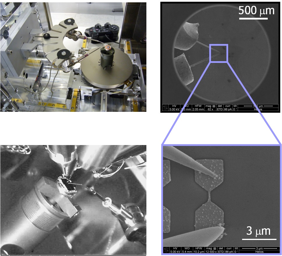
Lamellae preparation (Omniprobe® micromanipulator)

EBL: electron beam lithography (Raith® software/hardware)

Electrical microprobes (Kleindiek®)

Lamellae preparation (Omniprobe® micromanipulator)

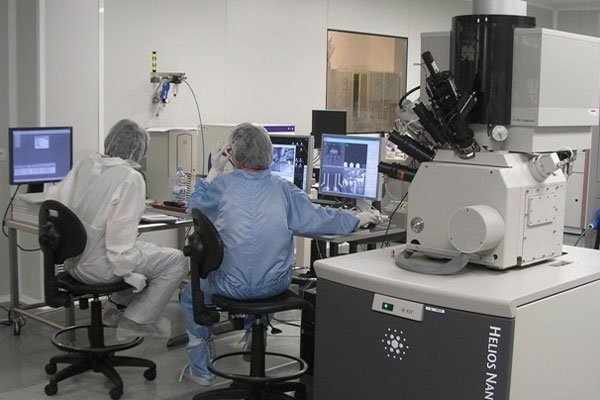
Laboratorio de Microscopías Avanzadas
We are a unique initiative at national and international levels. We provide the scientific and industrial community with the most advanced infrastructures in Nanofabrication, Local Probe and Electron Microscopies for the observation, characterization, nanopatterning and handling of materials at atomic and molecular scale.
Contact information
Campus Río Ebro, Edificio Edificio I+D+i

Direct Links
© 2021 LMA | Website developed by o10media | Política de privacidad | Aviso legal | Condiciones de uso | Política de Cookies |