

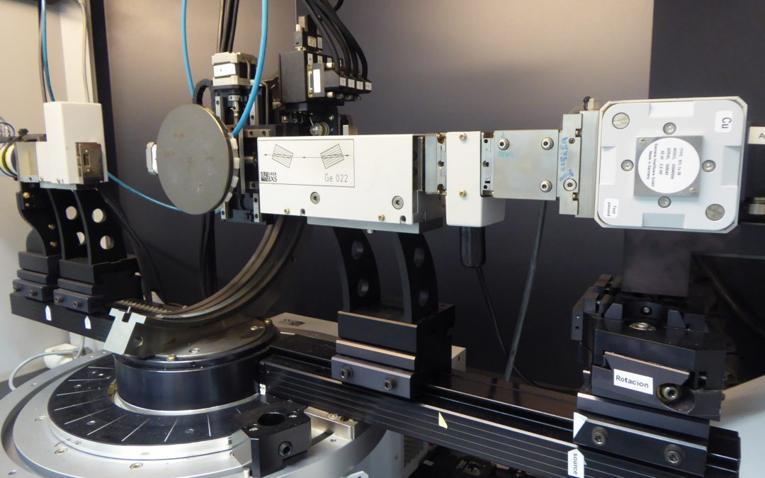
The equipment configuration is optimized for high-resolution X-ray diffraction (HR-XRD) and reflectivity (XRR) studies in nanostructured thin films and superlattices. For this purpose it includes incident and diffracted-beam monochromators, collimators, attenuators and eulerian sample holder. It also allows the local mapping of flat samples through motorized lateral displacements.

- High resolution diffraction in epitaxial films and multilayers
- Reciprocal space maps
- Wafer mapping
- X-ray reflectivity
- Structural characterization of single-crystal or strongly textured thin films
- Grazing incidence diffraction (GID)
The XRD equipment is mainly used by researchers growing epitaxial thin films in the following applications and research lines:
- Epitaxially strained thin films)
- Magnetic thin films and nanostructres for applications in Spintronics)
- Multiferroic films and multilayers)
- Thin films showing thermoelectric effects (such as spin Seebeck)
The expertise of our scientific and technical staff is also offered to researchers from public and private research centers and also to professionals from industrial sectors that require the use of this instrument.


SrRuO3/BaTiO3 heterostructure grown on a GdScO3 substrate.
- Chemical composition
- Crystal structure
- Lattice parameters
- Substrate and film orientation
- Miscut angle in single-crystal substrates
- Crystalline quality and texture
- Roughness
- Density
- Thickness
- Defects, dislocations
- Stress
- X-ray generator with copper anode
- (022) Ge monochromator (Cu Ka1 line)
- Parallel-beam optics (Göbel mirror)
- Eulerian cradle and XYZ translation stage
- Zeta and Xi tilt stage for grazing incidence X-ray diffraction
- Suction device for securing flat samples
- Soller slits
- X-ray beam intensity attenuator
- Automatic alignment control by microscope and laser beam
- Scintillation counter
- Analysis software and databases
Laboratorio de Microscopías Avanzadas
We are a unique initiative at national and international levels. We provide the scientific and industrial community with the most advanced infrastructures in Nanofabrication, Local Probe and Electron Microscopies for the observation, characterization, nanopatterning and handling of materials at atomic and molecular scale.
Contact information
Campus Río Ebro, Edificio Edificio I+D+i

Direct Links
© 2021 LMA | Website developed by o10media | Política de privacidad | Aviso legal | Condiciones de uso | Política de Cookies |