

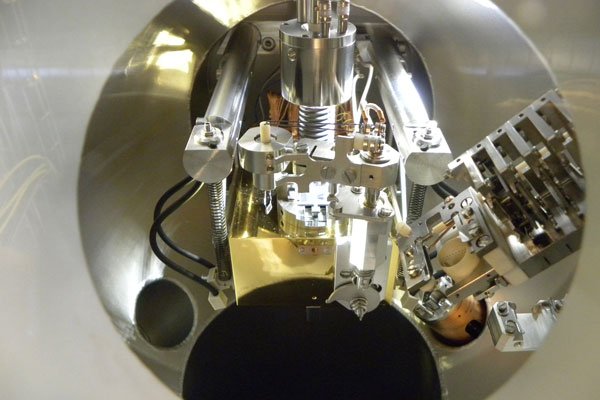
The Aahrus is a combined STM and non-contact AFM head which operates a KolibriTM sensor under Ultra-high-vacuum conditions (P<10-10 mbar). Apart from allowing for imaging of metallic and insulating samples with atomic resolution, its unique feature is a radiative filament which can heat the sample up to 900ºC while keeping the tip and scanner protected near room temperature. This accessory, together with the possibility of dosing gases and evaporating materilas in-situ during scanning, makes the Aahrus an excellent instrument to explore the real-time chemical and catalytical activity of a surface by bringing the system to artificial thermodynamic conditions which can be tuned to the particular time resolution required for each experiment.
The microscope is connected under UHV conditions to the JT-STM facility, which offers all kind of sample preparation accessories and allows users to exchange the very same sample between both microscopes. The Aahrus is regularly applied to real-time monitoring of thermally activated processes such as chemical vapour deposition (for instance graphene growth on metallic surfaces), on-surface synthesis, metal epitaxy and self-assembled organic monolayers.

Scanning Probe Microscopy and spectroscopy:
- Structural characterization with atomic resolution of metallic and insulating surfaces.
- Fast loading approach and flexible design for quick characterization of samples grown in-situ or taken as-prepared from the outside.
- Force spectroscopy with sub-Å Z resolution
- Chemical contrast mapping with atomic resolution using repulsive or attracting tip-atom forces.
- Dedicated Kelvin Probe Microscopy module.
Real-time physical-chemical characterization of 2D materials:
- Real-time monitoring of surface dynamics up to 900 ºC
- Controlled gas-dosing in-situ during scanning.
- Capable of scanning during evaporation of organic or inorganic materials.
-
Temperature range: 100 (LN2 flow cryostat) to 1200 K (radiative heater)
-
LN2 hold time: 24 hours
-
Z topographic noise: 5 pm peak-peak; <2000 fm/ÖHz
-
Thermal drift at low temperatures: Standard STM grade images can be obtained with scan time <5 min at temperatures <250 K.
-
Thermal drift at high temperatures: For T<600 ºC standard STM grade images can be obtained after thermal relaxation of about 15 min. For 600 ºC < T < 900 ºC scan time is limited to 5-10 minutes.
-
Minimum stable oscillation amplitude of Kolibri sensor for nc-AFM: 90 pm
-
Force resolution: <1 pN
-
Maximum operating pressure: 1´10-5 mbar.
-
In-situ tip conditioning
(shared with SPECS JT-STM) 3 ion-guns, 3 e-beam heaters (100-1300ºC). 1 flash heater (>2000 ºC in 25 seconds), low energy electron diffraction and Auger spectroscopy (SPECS ErLEED 150), quadrupole mass spectrometer for residual gas analysis, 7 leak-valves for controlled gas injection, 1 SPECS EBE4 and 1 SPECS EBE1 e-beam evaporators, 2 parking stations for mini-UHV transportable organic evaporators, 1 high temperature effusion cell (CreaTec)

Atomically resolved Ag(111) surface in nc-AFM mode. Kolibri PLL parameters nres~1 MHz, Q~25000, oscillation amplitude 200 pm, DnSP=0.2 Hz (positive feedback range), 2 lines/second.

Fig 2. Sequential set of images of Tm/W(110) while increasing the temperature. At RT an amorphous deposit is obtained. At 400ºC the Tm atoms arrange epitaxially over the W(110) forming a Moirée patter. At 750-800 ºC WC are segregated from where the Tm is expelled. At 900ºC the Tm desorbs and the bare W(110) surface remains.

ig 3. Time evolution of CVD of propene on Ni(111) at 550 ºC. After taking the left-most frame showing a clean Ni surface with fuzzy step edges due to the atoms mobility at this temperature, a partial pressure of propene of 110-6 mbar is dosed into the chamber. The second panel shows the formation front of a Ni2C monolayer. After a few minutes the whole scan area is covered by Ni2C (as confirmed by the atomically resolved images in the right panel), where the atomic steps have been wiped out due to microscale mass transport of Ni to accommodate the lower density phase of the product.
Laboratorio de Microscopías Avanzadas
We are a unique initiative at national and international levels. We provide the scientific and industrial community with the most advanced infrastructures in Nanofabrication, Local Probe and Electron Microscopies for the observation, characterization, nanopatterning and handling of materials at atomic and molecular scale.
Contact information
Campus Río Ebro, Edificio Edificio I+D+i

Direct Links
© 2021 LMA | Website developed by o10media | Política de privacidad | Aviso legal | Condiciones de uso | Política de Cookies |