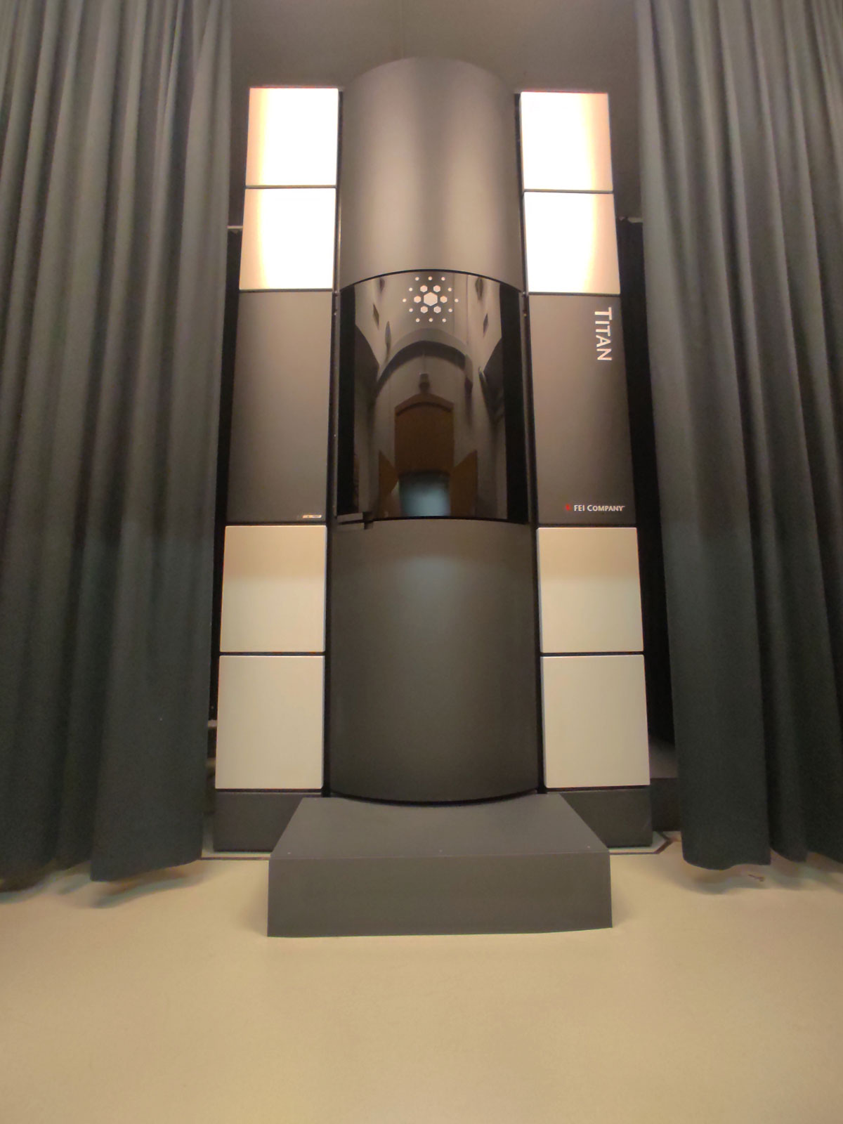
3Following its latest upgrade, our Titan Image microscope now features a double corrector system: one for the objective lens (CETCOR) and one for the condenser lens (Cs DCOR). This enables us to obtain ultra-high-resolution images in both TEM mode (HRTEM) and STEM mode (HRSTEM). It is also equipped with a biprism and a Lorentz lens for magnetic holography and high-resolution Lorentz microscopy.
Specialized software and sample holders are available for TEM and STEM tomography and 3D imaging. In addition, a segmented detector allows for iDPC imaging and the capability to perform 4D-STEM using the CETA camera.
A monochromator has also been added, along with a high-brightness field emission gun (XFEG), which makes it particularly suitable for EELS analysis using the new energy filter, GIF Continuum 1069 (80–300) FXUP. We have also incorporated a Super-X G2 EDS detector for EDS analysis.
The working voltages for this microscope are 30, 80, and 300 kV. The ability to operate at low voltages (30 kV, 80 kV) allows the corrector to achieve high resolution even on highly electron beam-sensitive materials such as graphene, carbon or heteroatom nanotubes, zeolites, mesoporous materials, and others.
Researchers from public or private institutions, as well as professionals from industry who require the use of this equipment, will also have access to the scientific and technical support of our highly qualified and experienced staff.

Imaging (Resolution: 0.08 nm)
- Morphology and size information of the material (TEM).
- Crystalline structure (electron diffraction, ultra-high-resolution TEM and STEM: HR(S)TEM).
- Sample composition information: scanning transmission imaging with high-angle annular dark field detector (STEM-HAADF).
- Energy-filtered transmission electron microscopy (EFTEM) images providing element-specific information.
Chemical Analysis
- X-ray spectroscopy (EDS) and Electron Energy Loss Spectroscopy (EELS).
- Atomic-resolution composition maps and profiles in scanning transmission mode (STEM).
- Light element analysis using iDPC.
Field Analysis
- Magnetic and electric field studies via electron holography.
- Magnetic domain studies: Lorentz microscopy.
- Stress/strain field studies through high-resolution image analysis.
In Situ Measurements
- Crystalline phase changes (electron diffraction).
- Defect structure analysis via bright field/dark field imaging (BF/DF) and weak-beam dark field (WBDF).
The new Titan Image microscope includes both image and probe correctors and operates at voltages ranging from 30 to 300 kV. It features a dynamic magnetic field compensator. The system is equipped with an X-FEG field emission gun and a 4k x 4k CETA camera for high-resolution image acquisition (HRTEM). The main working techniques include:
- HRTEM: For high-resolution imaging (HRTEM), the Titan Image microscope is equipped with a SuperTwin® objective lens and a spherical aberration corrector (CETCOR, CEOS Company), allowing an image resolution of 0.08 nm.
- HRSTEM: The microscope includes a scanning module for corrected STEM mode with a DCOR detector and BF (bright field), DF (dark field), and HAADF (high-angle annular dark field) detectors, enabling an image resolution of 0.05 nm.
- iDPC: Imaging of light elements using a segmented annular detector.
- EDS: The Super-X G2 EDS detector enables fast EDS mapping with a higher count rate and no limitations related to sample orientation.
- EELS: The Gatan Continuum K3 HR/1069HR (80–300 kV) energy filter with FXUP (60–300 kV) includes a direct detection K3 camera (3.4k x 3.4k). Together with the X-FEG gun and the monochromator (ulti-mono option), it enables an energy resolution of ~0.014 eV.
- Lorentz Microscopy and Holography: The microscope is also equipped with a Lorentz lens and an electrostatic biprism for the analysis of magnetic materials.
- Tomography: Dedicated software and sample holders for 3D reconstruction and compositional 3D mapping.

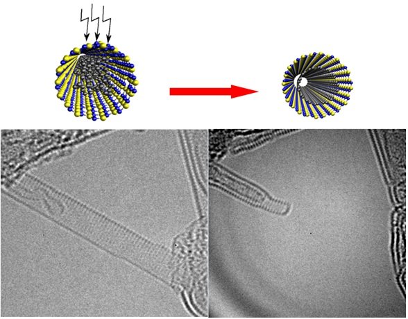
In Situ Formation of Carbon Nanotubes Encapsulated within Boron Nitride Nanotubes via Electron Irradiation Ref.: ACS Nano 8, 8419-8425 (2014) doi:10.1021/nn502912w

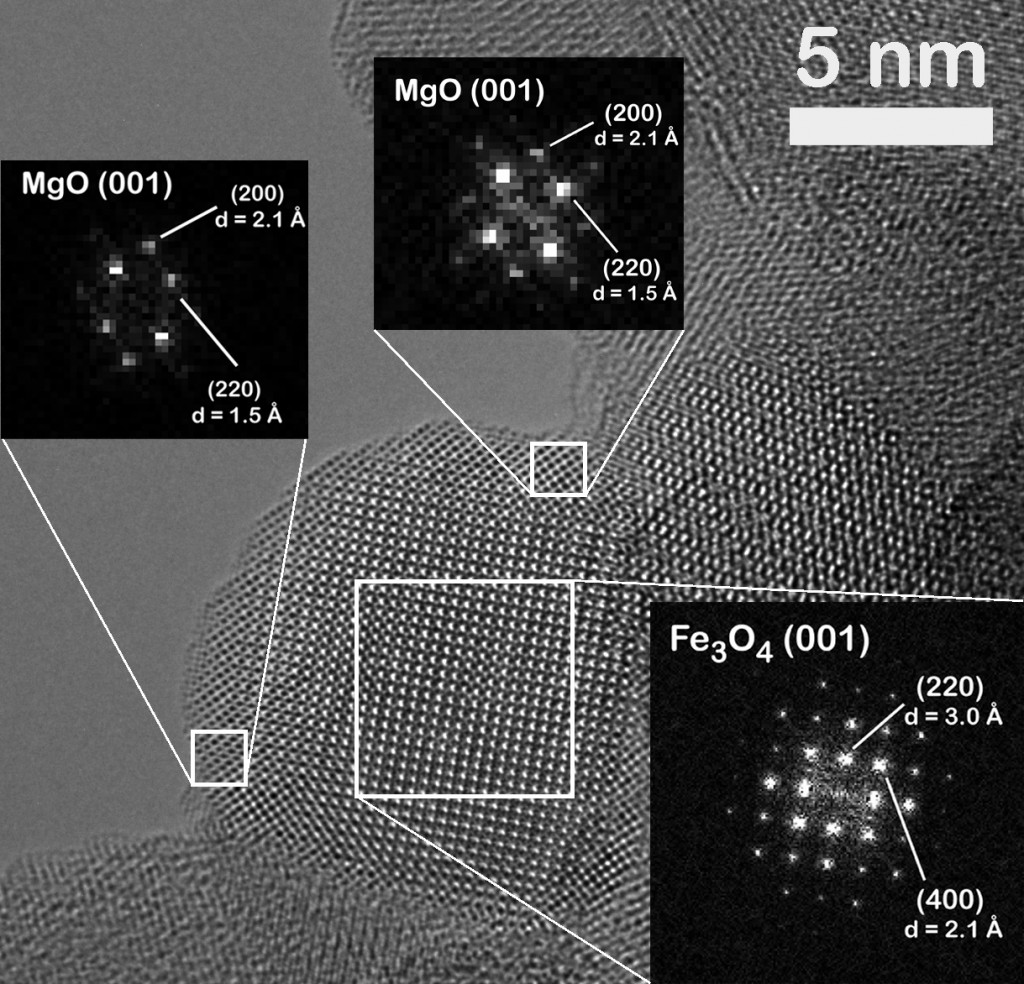
Aberration corrected HRTEM image of a magnetite nanoparticle epitaxially coated by a 1-nm-thick MgO layer. The insets show the FFT calculated from the areas marked with white squares. Ref.: Chem. Mater., 2012, 24 (3), pp 451–456. doi:10.1021/cm202306z
Laboratorio de Microscopías Avanzadas
We are a unique initiative at national and international levels. We provide the scientific and industrial community with the most advanced infrastructures in Nanofabrication, Local Probe and Electron Microscopies for the observation, characterization, nanopatterning and handling of materials at atomic and molecular scale.
Contact information
Campus Río Ebro, Edificio Edificio I+D+i
Direct Links
© 2021 LMA | Website developed by o10media | Política de privacidad | Aviso legal | Condiciones de uso | Política de Cookies |


