

X-Ray photoelectron spectroscopy (XPS) is a surface-sensitive quantitative spectroscopic technique mainly used to analyse the surface chemistry of a material. XPS it is one of the most powerful techniques for the study of surfaces, interfaces and thin films. During an XPS analysis a sample is irradiated with a monochromatic x-ray beam, resulting in the emission of photoelectrons whose energies are characteristic of the elements and their oxidation state within the sampling volume.
XPS is routinely used in the characterization of polymers, alloys, semiconductors, minerals, inks, adhesives, inorganic materials, glass, thin films, etc. and to study surface effects/process as segregation, diffusion, adsorption/desorption, corrosion, degradation, adhesion, soldering, contamination, cleaning, coating, functionalization, etc.

- Technical specifications
- Other electron spectroscopies for surface analysis implemented in the spectrometers
- Areas of interest
- Sample requirements
- Thechnical specifications and capabilities
1. Chemical composition. Qualitative and quantitative elemental analysis.
Highly surface sensitive (top 3-10nm)
Sensitive to elements with Z≥2 (Li→ ). Excellent specificity.
Sensitivity: 0.1 – 1% atomic
Typical quantification error: ~10%
2. Oxidation states. Qualitative and quantitaive analysis of chemical species.
3. Lateral distribution of chemical composition (elements & oxidation states). Image.
Spatial resolution in the order of microns.
4. Depth profiling. Chemical composition, thickness of coatings, functionalized layers and oxide layers.
ARXPS (Angle resolves XPS) < 10nm. Non destructive
Ar ion sputtering (mono-ion / clusters). 102 – 103 nm. Destructive
1. Ultraviolet photoelectron Spectroscopy (UPS): UPS uses UV radiation instead of X-Rays and so photoelectrons are excited from outer electronic levels (Valence Band). More Surface sensitive than XPS. Analysis of Valence Band, Fermi Level, determination of Work Function…
-
Thin films and coatings.
-
Surface functionalization.
-
Polymers and adhesives.
-
Mineralogy, geochemistry, and petrochemistry.
-
Metallurgy.
-
Catalysis.
-
Microelectronics and semiconductors.
… and other area requiring surface characterization of solids.
Any sample (conductive, non‐conductive, magnetic, organic, inorganic, powder, bulk, viscous…) provided it is compatible with high vacuum.
- There is no need of any specific sample preparation or coating process.
- Maximum dimensions dependent upon used sample-holder and analysis chamber geometry. Maximum diameter 32 x 75 mm. Maximum thickness 7mm (up to 13 mm depending on the diameter)
- Non‐destructive analysis (X-Ray are capable to induce some changes or degradation in some materials)
- Sampled area (analysis spot): from 15 μm (minimum) – 700 μm (standard).
- Analysis depth: 3 – 10 nm (higher is possible by etching).
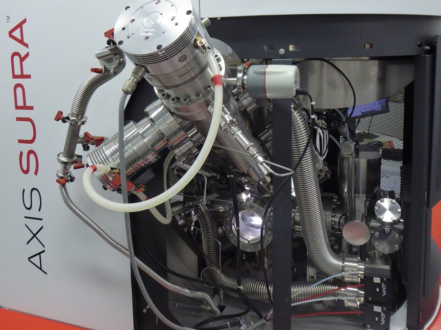
X-Ray sources for XPS
- Al-Monochromatic (1486.6 eV)
- Ag- Monochromatic (2984.2 eV)
UV lamp for UPS
- HeI (21.22 eV)
- HeII (40.80 eV)
Mono Ar+ ion gun and gas cluster Argon ion source 20kV (GCIS) for cleaning and depth profiling
166 mm diameter Hemispherical Energy Analyser (HSA) for high sensitivity and high resolution spectroscopy (FWHM) Ag3d5/2 <0.48eV)
Spherical Mirror Analyser (SMA) for parallel imaging with real time data acquisition of chemical images
Multichannel DLD detector
- Spatial resolution 15 µm (spectroscopic mode) and 1 µm (parallel image mode)
- Sample stage with 5 displacement axis including Theta rotation for ARXPS and Zalar rotation for optimum depth profiles.
- Charge Neutralizer for non-conducting samples: flood electron gun
- Analysis Software (ESCApe & CasaXPS) and Data Bases

Martín et al. Chem. Eur. J. 2014, 20, 3421.

Lucía González et al. Chem. Mater., 2013, 25 (22), pp 4503–4510

Mizrahi et al. Langmuir 29 (2013) 10087-10094

Ballesteros et al. Langmuir 2011, 27, 3600–3610

Fig. 5 Mafalda Rodrigues et al. Adv. Funct. Mater. 2016, 26, 200-209
Advanced Microscopy Laboratory
We are a unique initiative at the national and international level. We provide the scientific and industrial community with the most advanced infrastructures in electron microscopy and local probe microscopy for the observation, characterization, nanostructuring and manipulation of materials at the atomic and molecular scale.
Contact information
Campus Río Ebro, Edificio Edificio I+D+i

Direct Links
© 2021 LMA | Website developed by o10media | Política de privacidad | Aviso legal | Condiciones de uso | Política de Cookies |