

This microscope has a monochromator and a High Brightness source (XFEG), which makes it ideal to determine optical properties by low-loss EELS as well as oxidation states studies by core-loss EELS and observation of the fine structure of the energy absorption edges by Energy Loss Near Edge Spectroscopy (ELNES).
Working at low-voltages (60 kV, 80 kV), and because of the aberration corrector, high resolution images can be obtained even on beam-sensitive materials such as graphene, carbon nanotubes, zeolites and mesoporous materials, etc.
The working voltages for this instrument are: 60, 80, 120, 200 and 300 kV.
The expertise of our scientific and technical staff is also offered to researchers from public and private research centers and also to professionals from industrial sectors that require the use of this instrument.

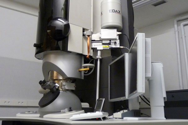
This Scanning Transmission Electron Microscope works either in TEM or in STEM modes at voltages between 60 and 300 kV. It can be used at low voltage to analyse electron irradiation sensitive materials. It is fitted with the last generation of a high brightness Schotky emitter developed by FEI (the so called “X-FEG” gun), a monochromator, and a Gatan 2k x 2k CCD camera. The main working techniques are:
- STEM: As this microscope is devoted for STEM and EELS experiments, it is equipped with a CESCOR Cs-probe corrector from CEOS Company allowing for the formation of an electron probe of 0.09 nm mean size. The TEM is equipped with all the STEM facilities (BF, DF, ADF and HAADF detectors) and 0.09 nm spatial resolution has indeed been achieved in STEM-HAADF mode. It is equipped with bright field (BF), dark field (DF) and high angle annular (HAADF) detectors.
- EELS and EDS: For EELS experiments, the microscope is fitted with a Gatan Energy Filter Tridiem 866 ERS and a monochromator. An energy resolution of 0.14 eV can be achieved with this setup. Combined with STEM mode, chemical composition maps and profiles with atomic resolution can be obtained. In November 2020 a new Energy Dispersive X-Ray Spectroscopy spectrometer (Oxford Instruments Ultim Max TLE 100) was installed at the column of the probe-corrected Titan (Thermofisher, formerly FEI). The acquistion of this new EDS spectrometer means a significant improvement in measurement sensitivity, and hence a great decrease in time of analysis. As a consequence, the obtained composition profiles and maps are much more accurate and precise, even for element concentrations below 1%, also for electron beam-sensitive materials. Besides, this new spectrometer enables the acquisition of atomic-resolved EDS. Also, since it is a windowless detector, it yields a higher sensitivity for the analysis of light elements, such as lithium, boron or carbon. Because of all the forementioned technical details, the analytical capabilities of the probe-corrected Titan have been notably improved.
- Lorentz and holography: in addition to the above described analytical capabilities, the Titan STEM corrected microscope is fitted with a Lorentz lens and an electrostatic biprism allowing Lorentz and medium resolution electron holography experiments to be carried out in a field-free environment (as needed for magnetic materials studies).
- Tomography: a tomography set-up with a +/- 70° single tilt stage permits to perform 3D reconstructions either in TEM or STEM modes.
Image (0.08 nm resolution)
- Size, morphology and crystalline structure information (TEM and STEM modes, electron diffraction). The contrast in the image depends on the atomic number (Z-contrast). Energy Filtered TEM (EFTEM) yields information about a specific element. Composition: Scanning-Transmission imaging with a High Angle Annular Dark Field detector (STEM-HAADF).
- Three dimensional (3D) reconstruction: electron tomography.
Chemical Analysis :
- X-Ray (EDS) and Electron Energy Loss Spectroscopies (EELS).
- Combined with the STEM mode: chemical composition with spatial resolution; composition maps and profiles with atomic resolution.
Vector Field Analysis
- Electric and magnetic field studies by Electron Holography.
- Magnetic domain studies by Lorentz Microscopy.
- Stress and strain studies by HRTEM imaging.
In-Situ physical properties measurements
- Changes of crystalline phase (Electron diffraction).
- Defect structure by bright field/dark field imaging (BF/DF) and Weak Beam imaging (WBDF).
Examples of work that can be done on this microscope:
1) Imagen HRSTEM
https://lma.unizar.es/en/carbon-based-materials/
https://lma.unizar.es/en/nanoparticles-and-nanomaterials/
https://lma.unizar.es/en/interface-heterostructures/
2) EDS and EELS Spectroscopic
https://lma.unizar.es/en/carbon-based-materials/
https://lma.unizar.es/en/nanoparticles-and-nanomaterials/
https://lma.unizar.es/en/interface-heterostructures/
3) Electronic tomography
https://lma.unizar.es/en/nanoparticles-and-nanomaterials/

(a) Z-contrast images along a particular planar defect of a YBCO nanocomposite. (b) exx deformation map showing in colors (red and green) different deformation values. Ref.: Appl. Phys. Lett. 102, 081906 (2013)
doi:10.1063/1.4793749

a) Ball-and-stick model, shown in perspective, of the Cd-loaded zeolite A. Cd in violet, O in red, and Si and Al in blue. b) Cs-corrected STEM image of a CdA. The FFT inset was indexed assuming Pm3m. Ref.: J. Phys. Chem. C, 2013, 117 (46), pp 24485–24489
http://pubs.acs.org/doi/abs/10.1021/jp409171q
Laboratorio de Microscopías Avanzadas
We are a unique initiative at national and international levels. We provide the scientific and industrial community with the most advanced infrastructures in Nanofabrication, Local Probe and Electron Microscopies for the observation, characterization, nanopatterning and handling of materials at atomic and molecular scale.
Contact information
Campus Río Ebro, Edificio Edificio I+D+i

Direct Links
© 2021 LMA | Website developed by o10media | Política de privacidad | Aviso legal | Condiciones de uso | Política de Cookies |